Semiconductor Electronics

119 Questions Start NEET Test
2026 Q1 NEET MCQ
08 May 2026

The current / in the circuit shown below is: (All diodes are ideal and identical)

NEET 2026 Physics - Semiconductor Electronics Question 5 English

A.

$\frac{5}{3} \mathrm{~A}$

B.

$\frac{5}{9} \mathrm{~A}$

C.

$\frac{1}{3} \mathrm{~A}$

D.

$\frac{15}{2} \mathrm{~A}$

2026 Q2 NEET MCQ
08 May 2026

$ \text { In the circuit shown below, the voltage appearing across the diode } D \text { will be of the form: } $

NEET 2026 Physics - Semiconductor Electronics Question 4 English

A.

NEET 2026 Physics - Semiconductor Electronics Question 4 English Option 1

B.

NEET 2026 Physics - Semiconductor Electronics Question 4 English Option 2

C.

NEET 2026 Physics - Semiconductor Electronics Question 4 English Option 3

D.

NEET 2026 Physics - Semiconductor Electronics Question 4 English Option 4

2026 Q3 NEET MCQ
08 May 2026

Two statements are given below:

A. When the forward bias voltage across a p-n junction diode increases above a certain threshold voltage, the diode current increases significantly.

B. This current is called reverse saturation current.

Choose the correct answer from the options given below:

A.

Both Statements A and B are true

B.

Statement A is true, but Statement B is false

C.

Both Statements $A$ and $B$ are false

D.

Statement A is false, but Statement B is true

2026 Q4 NEET MCQ
28 Jun 2026

An ideal Zener diode with breakdown voltage of -3 V is reverse biased with a negative input voltage $V_i=-5 \mathrm{~V}$. The magnitude of voltage difference between point $B$ and $A$ is:

RE-NEET 2026 Physics - Semiconductor Electronics Question 2 English

A.

0 V

B.

3 V

C.

2 V

D.

1 V

2026 Q5 NEET MCQ
28 Jun 2026

Three identical p-n junction diodes $D_1, D_2$, and $D_3$ are connected across a battery as shown in the figure. If the width of the depletion regions of $D_1, D_2$ and $D_3$ are $W_1, W_2$ and $W_3$, respectively, then the correct option is:

RE-NEET 2026 Physics - Semiconductor Electronics Question 1 English

A.

$W_2>W_1=W_3$

B.

$W_1>W_2>W_3$

C.

$ W_3=W_1>W_2$

D.

$ W_3>W_2>W_1$

2025 Q6 NEET MCQ
10 Mar 2026

A full wave rectifier circuit with diodes $\left(D_1\right)$ and $\left(D_2\right)$ is shown in the figure. If input supply voltage $\mathrm{V}_{\text {in }}=220 \sin (100 \pi t)$ volt, then at $t=15 \mathrm{msec}$

NEET 2025 Physics - Semiconductor Electronics Question 6 English

A.
$\quad D_1$ and $D_2$ both are forward biased
B.
$\quad D_1$ and $D_2$ both are reverse biased
C.
$\quad D_1$ is forward biased, $D_2$ is reverse biased
D.
$\quad D_1$ is reverse biased, $D_2$ is forward biased.
2025 Q7 NEET MCQ
10 Mar 2026

The output ( $Y$ ) of the given logic implementation is similar to the output of an/a ________ gate.

NEET 2025 Physics - Semiconductor Electronics Question 7 English

A.
OR
B.
NOR
C.
AND
D.
NAND
2024 Q8 NEET MCQ
10 Mar 2026

NEET 2024 (Re-Examination) Physics - Semiconductor Electronics Question 9 English

The I-V characteristics shown above are exhibited by a

A.
Light emitting diode
B.
Zener diode
C.
Photodiode
D.
Solar cell
2024 Q9 NEET MCQ
10 Mar 2026

When the output of an OR gate is applied as input to a NOT gate, then the combination acts as a

A.
NAND gate
B.
NOR gate
C.
AND gate
D.
OR gate
2024 Q10 NEET MCQ
10 Mar 2026

The output Y for the inputs A and B of the given logic circuit is:

NEET 2024 (Re-Examination) Physics - Semiconductor Electronics Question 8 English

A.
$A \cdot B$
B.
$\bar{A} \cdot \bar{B}$
C.
$A+B$
D.
$\bar{A}+\bar{B}$
2024 Q11 NEET MCQ
10 Mar 2026

A logic circuit provides the output $Y$ as per the following truth table :

NEET 2024 Physics - Semiconductor Electronics Question 12 English

The expression of the output Y is :

A.
$ A \cdot B+\bar{A} $
B.
$ A \cdot \bar{B}+\bar{A} $
C.
$ \bar{B} $
D.
B
2024 Q12 NEET MCQ
10 Mar 2026

Consider the following statements A and B and identify the correct answer :

NEET 2024 Physics - Semiconductor Electronics Question 11 English

A. For a solar-cell, the I-V characteristics lies in the IV quadrant of the given graph.

B. In a reverse biased $p n$ junction diode, the current measured in $(\mu \mathrm{A})$, is due to majority charge carriers.

A.
$A$ is correct but $B$ is incorrect
B.
$A$ is incorrect but $B$ is correct
C.
Both A and B are correct
D.
Both $A$ and $B$ are incorrect
2024 Q13 NEET MCQ
10 Mar 2026

$ \text { The output ( } Y \text { ) of the given logic gate is similar to the output of an/a } $

NEET 2024 Physics - Semiconductor Electronics Question 13 English

A.
NAND gate
B.
NOR gate
C.
OR gate
D.
AND gate
2023 Q14 NEET MCQ
10 Mar 2026

On the basis of electrical conductivity, which one of the following material has the smallest resistivity?

A.
Germanium
B.
Silver
C.
Glass
D.
Silicon
2023 Q15 NEET MCQ
10 Mar 2026

The given circuit is equivalent to:

NEET 2023 Manipur Physics - Semiconductor Electronics Question 14 English

A.
NEET 2023 Manipur Physics - Semiconductor Electronics Question 14 English Option 1
B.
NEET 2023 Manipur Physics - Semiconductor Electronics Question 14 English Option 2
C.
NEET 2023 Manipur Physics - Semiconductor Electronics Question 14 English Option 3
D.
NEET 2023 Manipur Physics - Semiconductor Electronics Question 14 English Option 4
2023 Q16 NEET MCQ
10 Mar 2026

A p-type extrinsic semiconductor is obtained when Germanium is doped with:

A.
Antimony
B.
Phosphorous
C.
Arsenic
D.
Boron
2023 Q17 NEET MCQ
10 Mar 2026

NEET 2023 Manipur Physics - Semiconductor Electronics Question 17 English

The above figure shows the circuit symbol of a transistor. Select the correct statements given below:

(A) The transistor has two segments of p-type semiconductor separated by a segment of n-type semiconductor.

(B) The emitter is of moderate size and heavily doped.

(C) The central segment is thin and lightly doped.

(D) The emitter base junction is reverse biased in common emitter amplifier circuit.

A.
(C) and (D)
B.
(A) and (D)
C.
(A) and (B)
D.
(B) and (C)
2023 Q18 NEET MCQ
10 Mar 2026

Given below are two statements:

Statement I : Photovoltaic devices can convert optical radiation into electricity.

Statement II : Zener diode is designed to operate under reverse bias in breakdown region.

In the light of the above statements, choose the most appropriate answer from the options given below :

A.
Both Statement I and Statement II are incorrect.
B.
Statement I is correct but Statement II is incorrect.
C.
Statement I is incorrect but Statement II is correct.
D.
Both Statement I and Statement II are correct
2023 Q19 NEET MCQ
10 Mar 2026

A full wave rectifier circuit consists of two p-n junction diodes, a centre-tapped transformer, capacitor and a load resistance. Which of these components remove the ac ripple from the rectified output?

A.
p-n junction diodes
B.
Capacitor
C.
Load resistance
D.
A centre-tapped transformer
2023 Q20 NEET MCQ
10 Mar 2026

For the following logic circuit, the truth table is:

NEET 2023 Physics - Semiconductor Electronics Question 20 English

A.
A B Y
0 0 0
0 1 1
1 0 1
1 1 1
B.
A B Y
0 0 1
0 1 0
1 0 1
1 1 0
C.
A B Y
0 0 0
0 1 0
1 0 0
1 1 1
D.
A B Y
0 0 1
0 1 1
1 0 1
1 1 0
2022 Q21 NEET MCQ
10 Mar 2026

NEET 2022 Phase 2 Physics - Semiconductor Electronics Question 23 English

Identify the equivalent logic gate represented by the given circuit

A.
NAND
B.
OR
C.
NOR
D.
AND
2022 Q22 NEET MCQ
10 Mar 2026

The incorrect statement about the property of a Zener diode is :

A.
p and n regions of Zener diode are heavily doped
B.
Zener voltage remains constant at breakdown
C.
It is designed to operate under reverse bias
D.
Depletion region formed is very wide
2022 Q23 NEET MCQ
10 Mar 2026

The collector current in a common base amplifier using n-p-n transistor is 24 mA. If 80% of the electrons released by the emitter is accepted by the collector, then the base current is numerically :

A.
3 mA and entering the base
B.
6 mA and leaving the base
C.
3 mA and leaving the base
D.
6 mA and entering the base
2022 Q24 NEET MCQ
10 Mar 2026

NEET 2022 Phase 1 Physics - Semiconductor Electronics Question 24 English

In the given circuits (a), (b) and (c), the potential drop across the two p-n junctions are equal in

A.
Circuit (a) only
B.
Circuit (b) only
C.
Circuit (c) only
D.
Both circuits (a) and (c)
2022 Q25 NEET MCQ
10 Mar 2026

As the temperature increases, the electrical resistance

A.
Increases for both conductors and semiconductors
B.
Decreases for both conductors and semiconductors
C.
Increases for conductors but decreases for semiconductors
D.
Decreases for conductors but increases for semiconductors
2022 Q26 NEET MCQ
10 Mar 2026

In half wave rectification, if the input frequency is 60 Hz, then the output frequency would be

A.
Zero
B.
30 Hz
C.
60 Hz
D.
120 Hz
2022 Q27 NEET MCQ
10 Mar 2026

NEET 2022 Phase 1 Physics - Semiconductor Electronics Question 26 English

The truth table for the given logic circuit is

A.
NEET 2022 Phase 1 Physics - Semiconductor Electronics Question 26 English Option 1
B.
NEET 2022 Phase 1 Physics - Semiconductor Electronics Question 26 English Option 2
C.
NEET 2022 Phase 1 Physics - Semiconductor Electronics Question 26 English Option 3
D.
NEET 2022 Phase 1 Physics - Semiconductor Electronics Question 26 English Option 4
2021 Q28 NEET MCQ
10 Mar 2026
Consider the following statements (A) and (B) and identify the correct answer.

(A) A Zener diode is connected in reverse bias, when used as a voltage regulator.

(B) The potential barrier of p-n junction lies between 0.1 V to 0.3 V.
A.
(A) is incorrect but (B) is correct.
B.
(A) and (B) both are correct.
C.
(A) and (B) both are incorrect.
D.
(A) is correct and (B) is incorrect.
2021 Q29 NEET MCQ
10 Mar 2026
The electron concentration in an n-type semiconductor is the same as hole concentration in a p-type semiconductor. An external field (electric) is applied across each of them. Compare the currents in them.
A.
No current will flow in p-type, current will only flow in n-type
B.
Current in n-type = current in p-type
C.
current in p-type > current in n-type
D.
current in n-type > current in p-type
2021 Q30 NEET MCQ
10 Mar 2026
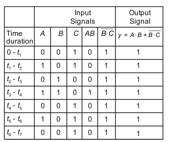
For the given circuit, the input digital signals are applied at the terminals A, B and C. What would be the output at the terminal y?

NEET 2021 Physics - Semiconductor Electronics Question 29 English 1 NEET 2021 Physics - Semiconductor Electronics Question 29 English 2
A.
NEET 2021 Physics - Semiconductor Electronics Question 29 English Option 1
B.
NEET 2021 Physics - Semiconductor Electronics Question 29 English Option 2
C.
NEET 2021 Physics - Semiconductor Electronics Question 29 English Option 3
D.
NEET 2021 Physics - Semiconductor Electronics Question 29 English Option 4
2020 Q31 NEET MCQ
10 Mar 2026
For transistor action, which of the following statements is correct?
A.
Base, emitter and collector regions should have same size.
B.
Both emitter junction as well as the collector junction are forwarded biased.
C.
The base region must be very thin and lightly doped.
D.
Base, emitter and collector regions should have same doping concentrations.
2020 Q32 NEET MCQ
10 Mar 2026
The increase in the width of the depletion region in a p-n junction diode is due to :
A.
reverse bias only
B.
both forward bias and reverse bias
C.
increase in forward current
D.
forward bias only
2020 Q33 NEET MCQ
10 Mar 2026
For the logic circuit shown, the truth table is :
NEET 2020 Phase 1 Physics - Semiconductor Electronics Question 32 English
A.
A B Y
0 0 0
0 1 1
1 0 1
1 1 1
B.
A B Y
0 0 1
0 1 1
1 0 1
1 1 0
C.
A B Y
0 0 1
0 1 0
1 0 0
1 1 0
D.
A B Y
0 0 0
0 1 0
1 0 0
1 1 1
2019 Q34 NEET MCQ
10 Mar 2026
The correct Boolean operation represented by the circuit diagram drawn is : NEET 2019 Physics - Semiconductor Electronics Question 38 English
A.
OR
B.
NAND
C.
NOR
D.
AND
2019 Q35 NEET MCQ
10 Mar 2026
For a p-type semiconductor, which of the following statements is true?
A.
Holes are the majority carriers and trivalent atoms are the dopants.
B.
Holes are the majority carriers and pentavalent atoms are the dopants.
C.
Electrons are the majority carriers and pentavalent atoms are the dopants
D.
Electrons are the majority carriers and trivalent atoms are the dopants.
2018 Q36 NEET MCQ
10 Mar 2026
In the circuit shown in the figure, the input voltage Vi is 20 V, VBE = 0 and VCE = 0. The values of IB , IC and $\beta $ are given by NEET 2018 Physics - Semiconductor Electronics Question 35 English
A.
IB = 40 $\mu $A, IC = 10 mA, $\beta $ = 250
B.
IB = 25 $\mu $A, IC = 5 mA, $\beta $ = 200
C.
IB = 20 $\mu $A, IC = 5 mA, $\beta $ = 250
D.
IB = 40 $\mu $A, IC = 5 mA, $\beta $ = 125
2018 Q37 NEET MCQ
10 Mar 2026
In the combination of the following gates the output Y can be written in terms of inputs A and B as NEET 2018 Physics - Semiconductor Electronics Question 36 English
A.
$\overline {A.B} $
B.
$A.\overline B + \overline A .B$
C.
$\overline {A.B} + A.B$
D.
$\overline {A + B} $
2018 Q38 NEET MCQ
10 Mar 2026
In a p-n junction diode, change in temperature due to heating
A.
affects only reverse resistance
B.
affects only forward resistance
C.
does not affect resistance of p-n junction
D.
affects the overall V - I characteristics of p-n junction
2017 Q39 NEET MCQ
10 Mar 2026
In a common emitter transistor amplifier the audio sgnal voltage across the collector is 3 V. The resistance of collector is 3 k$\Omega $. If current gain is 100 and the base resistance is 2 k$\Omega $, the voltage and power gain of the amplifier is
A.
15 and 200
B.
150 and 15000
C.
20 and 2000
D.
200 and 1000
2017 Q40 NEET MCQ
10 Mar 2026
The given electrical network is equivalent to

NEET 2017 Physics - Semiconductor Electronics Question 118 English
A.
OR gate
B.
NOR gate
C.
NOT gate
D.
AND gate
2017 Q41 NEET MCQ
10 Mar 2026
Which one of the following represents forward bias diode ?
A.
NEET 2017 Physics - Semiconductor Electronics Question 117 English Option 1
B.
NEET 2017 Physics - Semiconductor Electronics Question 117 English Option 2
C.
NEET 2017 Physics - Semiconductor Electronics Question 117 English Option 3
D.
NEET 2017 Physics - Semiconductor Electronics Question 117 English Option 4
2016 Q42 NEET MCQ
10 Mar 2026
What is the output Y in the following circuit, when all the three inputs A, B, C are first 0 and then 1 ?

NEET 2016 Phase 2 Physics - Semiconductor Electronics Question 113 English
A.
0, 1
B.
0, 0
C.
1, 0
D.
1, 1
2016 Q43 NEET MCQ
10 Mar 2026
The given circuit has two ideal diodes connected as shown in the figure. The current flowing through the resistance R1 will be

NEET 2016 Phase 2 Physics - Semiconductor Electronics Question 114 English
A.
2.5 A
B.
10.0 A
C.
1.43 A
D.
3.13 A
2016 Q44 NEET MCQ
10 Mar 2026
For CE transistor amplifier, the aufio signal voltage across the collector resistance of 2 k$\Omega $ is 4 V. If the current amplification factor of the transistor is 100 and the base resistance is 1 k$\Omega $, then the input signal voltage is
A.
10 mV
B.
20 mV
C.
30 mV
D.
15 mV
2016 Q45 NEET MCQ
10 Mar 2026
To get output 1 for the following circuit, the correct choice for the input is

NEET 2016 Phase 1 Physics - Semiconductor Electronics Question 112 English
A.
A = 1, B = 1, C = 0
B.
A = 1, B = 0, C = 1
C.
A = 0, B = 1, C = 0
D.
A = 1, B = 0, C = 0
2016 Q46 NEET MCQ
10 Mar 2026
A npn transistor is connected in common emitter configuration in a given amplifier. A load resistance of 800 $\Omega $ is connected in the collector circuit and the voltage frop across it is 0.8 V. If the current amplification factor is 0.96 and the input resistance of the circuit is 192 $\Omega $, the voltage gain and the power gain of the amplifier will respectively be
A.
4, 4
B.
4, 3.69
C.
4, 3.84
D.
3.69, 3.84
2016 Q47 NEET MCQ
10 Mar 2026
Consider the junction diode as ideal. The value of current flowing through AB is

NEET 2016 Phase 1 Physics - Semiconductor Electronics Question 110 English
A.
10$-$1 A
B.
10$-$3 A
C.
0 A
D.
10$-$2 A
2015 Q48 NEET MCQ
10 Mar 2026
The input signal given to a CE amplifier having a voltage gain of 150 is Vi = 2cos(15t + ${\pi \over 3}$). The corresponding output signal will be
A.
2cos$\left( {15t + {{5\pi } \over 6}} \right)$
B.
300cos$\left( {15t + {{4\pi } \over 3}} \right)$
C.
300cos$\left( {15t + {{\pi } \over 3}} \right)$
D.
75cos$\left( {15t + {{2\pi } \over 3}} \right)$
2015 Q49 NEET MCQ
10 Mar 2026
In the given figure, a diode D is connected to an external resistance R = 100 $\Omega $ and an e.m.f. of 3.5 V. If the barrier potential developed across the diode is 0.5 V, the current in the citcuit will be

AIPMT 2015 Physics - Semiconductor Electronics Question 108 English
A.
20 mA
B.
35 mA
C.
30 mA
D.
40 mA
2015 Q50 NEET MCQ
10 Mar 2026
Which logic gate is represented by the following combination of logic gates ?

AIPMT 2015 Cancelled Paper Physics - Semiconductor Electronics Question 107 English
A.
AND
B.
NOR
C.
OR
D.
NAND