Semiconductor Electronics
The current / in the circuit shown below is: (All diodes are ideal and identical)

$\frac{5}{3} \mathrm{~A}$
$\frac{5}{9} \mathrm{~A}$
$\frac{1}{3} \mathrm{~A}$
$\frac{15}{2} \mathrm{~A}$

$ \text { In the circuit shown below, the voltage appearing across the diode } D \text { will be of the form: } $


Two statements are given below:
A. When the forward bias voltage across a p-n junction diode increases above a certain threshold voltage, the diode current increases significantly.
B. This current is called reverse saturation current.
Choose the correct answer from the options given below:
Both Statements A and B are true
Statement A is true, but Statement B is false
Both Statements $A$ and $B$ are false
Statement A is false, but Statement B is true

An ideal Zener diode with breakdown voltage of -3 V is reverse biased with a negative input voltage $V_i=-5 \mathrm{~V}$. The magnitude of voltage difference between point $B$ and $A$ is:

0 V
3 V
2 V
1 V

Three identical p-n junction diodes $D_1, D_2$, and $D_3$ are connected across a battery as shown in the figure. If the width of the depletion regions of $D_1, D_2$ and $D_3$ are $W_1, W_2$ and $W_3$, respectively, then the correct option is:

$W_2>W_1=W_3$
$W_1>W_2>W_3$
$ W_3=W_1>W_2$
$ W_3>W_2>W_1$
A full wave rectifier circuit with diodes $\left(D_1\right)$ and $\left(D_2\right)$ is shown in the figure. If input supply voltage $\mathrm{V}_{\text {in }}=220 \sin (100 \pi t)$ volt, then at $t=15 \mathrm{msec}$

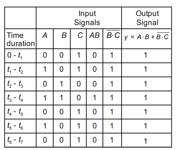
The output ( $Y$ ) of the given logic implementation is similar to the output of an/a ________ gate.


The I-V characteristics shown above are exhibited by a

When the output of an OR gate is applied as input to a NOT gate, then the combination acts as a
The output Y for the inputs A and B of the given logic circuit is:


A logic circuit provides the output $Y$ as per the following truth table :

The expression of the output Y is :
Consider the following statements A and B and identify the correct answer :

A. For a solar-cell, the I-V characteristics lies in the IV quadrant of the given graph.
B. In a reverse biased $p n$ junction diode, the current measured in $(\mu \mathrm{A})$, is due to majority charge carriers.

$ \text { The output ( } Y \text { ) of the given logic gate is similar to the output of an/a } $


On the basis of electrical conductivity, which one of the following material has the smallest resistivity?
The given circuit is equivalent to:


A p-type extrinsic semiconductor is obtained when Germanium is doped with:

The above figure shows the circuit symbol of a transistor. Select the correct statements given below:
(A) The transistor has two segments of p-type semiconductor separated by a segment of n-type semiconductor.
(B) The emitter is of moderate size and heavily doped.
(C) The central segment is thin and lightly doped.
(D) The emitter base junction is reverse biased in common emitter amplifier circuit.
Given below are two statements:
Statement I : Photovoltaic devices can convert optical radiation into electricity.
Statement II : Zener diode is designed to operate under reverse bias in breakdown region.
In the light of the above statements, choose the most appropriate answer from the options given below :
A full wave rectifier circuit consists of two p-n junction diodes, a centre-tapped transformer, capacitor and a load resistance. Which of these components remove the ac ripple from the rectified output?
For the following logic circuit, the truth table is:

| A | B | Y |
|---|---|---|
| 0 | 0 | 0 |
| 0 | 1 | 1 |
| 1 | 0 | 1 |
| 1 | 1 | 1 |
| A | B | Y |
|---|---|---|
| 0 | 0 | 1 |
| 0 | 1 | 0 |
| 1 | 0 | 1 |
| 1 | 1 | 0 |
| A | B | Y |
|---|---|---|
| 0 | 0 | 0 |
| 0 | 1 | 0 |
| 1 | 0 | 0 |
| 1 | 1 | 1 |
| A | B | Y |
|---|---|---|
| 0 | 0 | 1 |
| 0 | 1 | 1 |
| 1 | 0 | 1 |
| 1 | 1 | 0 |

Identify the equivalent logic gate represented by the given circuit
The incorrect statement about the property of a Zener diode is :
The collector current in a common base amplifier using n-p-n transistor is 24 mA. If 80% of the electrons released by the emitter is accepted by the collector, then the base current is numerically :


In the given circuits (a), (b) and (c), the potential drop across the two p-n junctions are equal in
As the temperature increases, the electrical resistance
In half wave rectification, if the input frequency is 60 Hz, then the output frequency would be

The truth table for the given logic circuit is


(A) A Zener diode is connected in reverse bias, when used as a voltage regulator.
(B) The potential barrier of p-n junction lies between 0.1 V to 0.3 V.


| A | B | Y |
|---|---|---|
| 0 | 0 | 0 |
| 0 | 1 | 1 |
| 1 | 0 | 1 |
| 1 | 1 | 1 |
| A | B | Y |
|---|---|---|
| 0 | 0 | 1 |
| 0 | 1 | 1 |
| 1 | 0 | 1 |
| 1 | 1 | 0 |
| A | B | Y |
|---|---|---|
| 0 | 0 | 1 |
| 0 | 1 | 0 |
| 1 | 0 | 0 |
| 1 | 1 | 0 |
| A | B | Y |
|---|---|---|
| 0 | 0 | 0 |
| 0 | 1 | 0 |
| 1 | 0 | 0 |
| 1 | 1 | 1 |


The given transistor operates in saturation region then what should be the value of $V_{B B}$ ?
$\begin{aligned} & \left(R_{\text {out }}=200 \Omega, R_{\text {in }}=100 \mathrm{~k} \Omega, V_{C C}=3 \mathrm{~V},\right. \\\\ & \left.V_{B E}=0.7 \mathrm{~V}, V_{C E}=0, \beta=200\right) \end{aligned}$

If voltage across a zener diode is 6V, then find out the value of maximum resistance in this condition.


Assertion : Photodiode and solar cell work on same mechanism.
Reason : Area is large for solar cell.


The diode used at a constant potential drop of 0.5 V at all currents and maximum power rating of 100 mW. What resistance must be connected in series diode, so that current in circuit is maximum?
Assertion Thickness of depletion layer is fixed in all semiconductor devices.
Reason No free charge carriers are available in depletion layer.


The current gain of a transistor in common emitter mode is 49. The change in collector current and emitter current corresponding to change in base current by $5.0 \mu \mathrm{A}$, will be
A specimen of silicon is to be made $P$-type semiconductor for this one atom of indium, on an average, is doped in $5 \times 10^7$ silicon atoms. If the number density of silicon is $5 \times 10^{22}$ atom/$\mathrm{m}^3$ then the number of acceptor atoms per $\mathrm{cm}^3$ will be
A proper combination of $3 \mathrm{NOT}$ and 1 NAND gates is shown. If $A=0, B=1, C=1$, then the output of this combination is


